Every electronics workbench has one—a drawer, box, or small organizer filled with components that you swear you identified earlier. A few resistors have faded color bands, capacitors have lost their labels, and there is always a collection of transistors and MOSFETs whose part numbers are just difficult enough to read that you end up reaching for your phone.
So the usual routine begins.
Pick up a component. Grab the multimeter. Check the resistance. Search the marking. Open a datasheet. Figure out the pinout. Test again. Then repeat the entire process for the next component.
A multimeter is indispensable on any electronics bench, but identifying an unknown component can become surprisingly tedious—especially when you are dealing with a mixed collection of resistors, capacitors, inductors, diodes, transistors and MOSFETs.
What if you could simply place the component into a tester, press one button, and let the instrument figure out what you are holding?
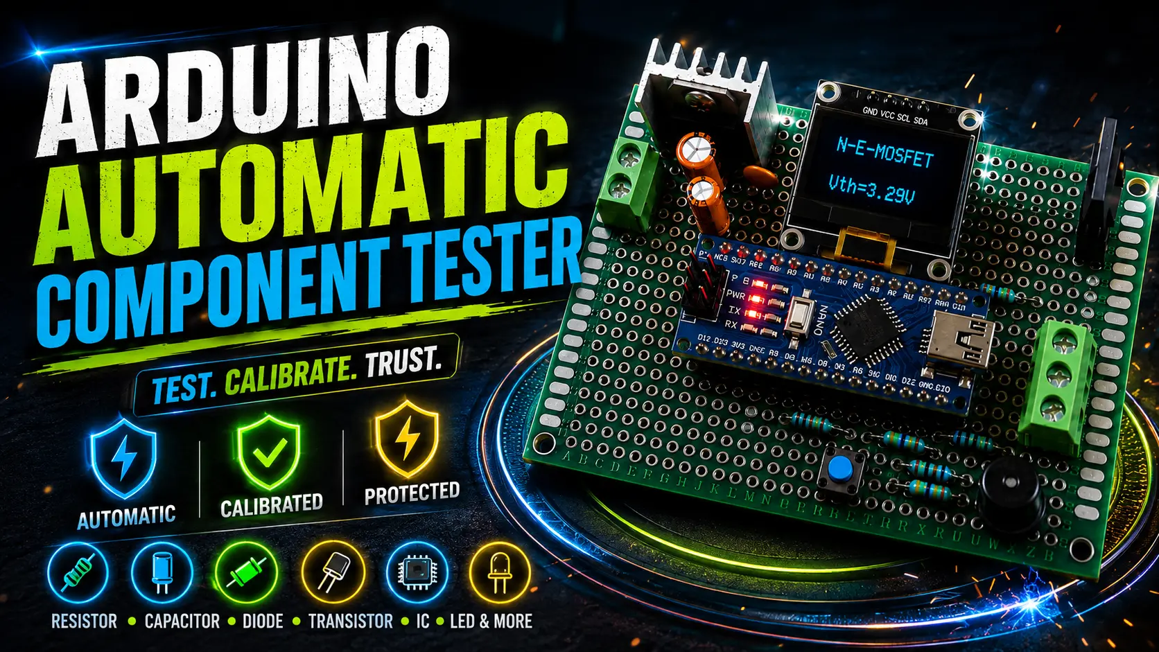
That is the idea behind this Arduino-based automatic component tester.
Instead of relying solely on component markings, the tester applies controlled measurement conditions to the device under test and analyzes its electrical behavior. The result is shown directly on an OLED display, allowing you to quickly identify components and view useful parameters such as resistance, capacitance, diode forward voltage, transistor hFE/VBE and MOSFET-related information. The firmware also performs automatic test-terminal checks and measurement routines to determine the appropriate component type.
And this isn’t designed simply as another bare Arduino experiment sitting on a breadboard. The goal is to turn the measurement system into a compact, practical bench instrument—complete with an OLED interface, dedicated test connections and a custom 3D-printed enclosure.
The result is a small tool that can sit beside your soldering iron and multimeter, ready to answer one of the most common questions in electronics:
“What component is this, and what is its actual value?”
What Is an Automatic Component Tester?
An automatic component tester uses a microcontroller to apply controlled electrical signals to an unknown component, measure its response through the ADC, and analyze the results to identify the component and estimate its value.
For example, the tester can measure resistance in a resistor, capacitance in a capacitor, forward voltage in a diode or LED, and parameters such as hFE and VBE in NPN/PNP transistors. The firmware also supports identification of various MOSFET and JFET types.
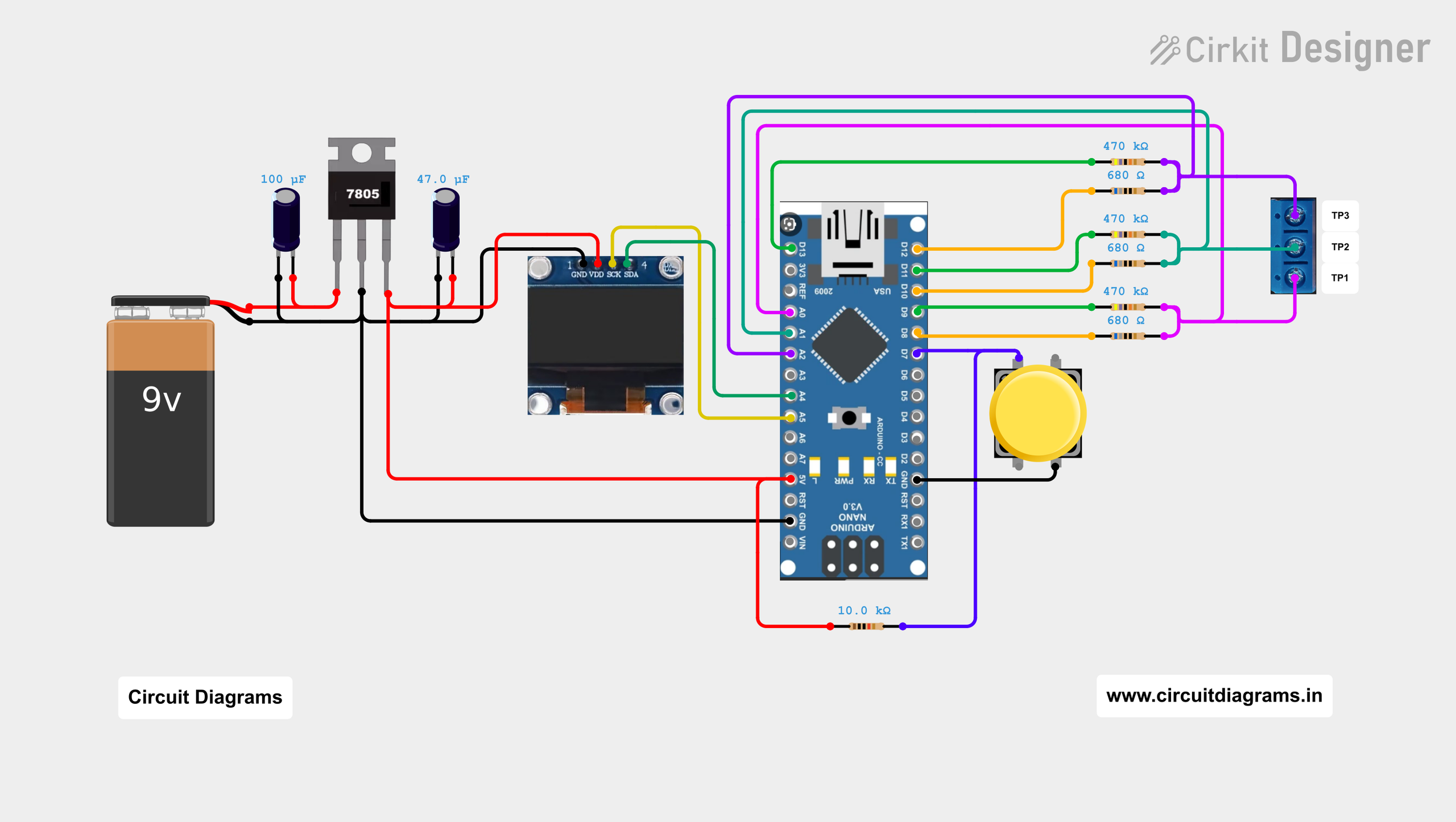
The project uses three test terminals—TP1, TP2 and TP3. Two-terminal components can be tested between different terminal combinations, while three terminals allow devices such as transistors and MOSFETs to be analyzed without requiring the user to know their pin arrangement beforehand.
It is important to remember that this is a DIY multi-purpose component tester, not a universal semiconductor analyzer. Its identification capabilities are limited to the component types and measurement routines implemented in the supplied firmware.
What This Arduino Component Tester Can Measure?
The firmware supports several major component categories, which can be divided into two-terminal components and three-terminal semiconductor devices.
Two-Terminal Components
- Resistors — measures resistance.
- Capacitors — measures capacitance.
- Inductors — measures inductance on supported configurations.
- Diodes & LEDs — identifies the diode junction and measures forward voltage.
Semiconductor Devices
- NPN & PNP Transistors — identifies the transistor type and measures parameters such as hFE and VBE.
- MOSFETs & JFETs — identifies different N-channel and P-channel FET types and provides relevant measurements.
The firmware contains dedicated detection and measurement routines for resistors, capacitors, inductors, diodes, transistors and FETs. It also includes support for additional semiconductor categories such as TRIACs and thyristors, although those are not part of the main practical testing section of this article.
Project Features
The project combines several useful functions into one compact instrument.
Key features include:
- Automatic component identification
- Resistor measurement
- Capacitor measurement
- Inductor measurement on supported configurations
- Diode forward-voltage measurement
- LED testing
- NPN/PNP transistor identification
- Transistor hFE and VBE measurement
- MOSFET/JFET identification
- 128×64 SSD1306 OLED
- Three-terminal component testing
- Reference-resistor calibration
- Automatic reference handling
- Charged-component detection
- Capacitor discharge routine
- Custom startup interface
- Compact 3D-printed enclosure
The firmware explicitly defines separate component modes for diode, transistor, FET, resistor, capacitor and other semiconductor categories.
So this isn’t simply an Arduino displaying ADC values. The firmware contains an actual measurement and identification system.
Circuit Diagram
Components Required
| Component | Quantity | Purpose |
|---|---|---|
| Arduino Nano / ATmega328P | 1 | Main microcontroller responsible for measurement, ADC processing and component identification. The firmware is designed around the ATmega328P. |
| 0.96-inch SSD1306 128×64 I²C OLED | 1 | Displays component type and measurement results. The firmware uses I²C address 0x3C. |
| Test terminals / component socket / test probes | 3 connections | Provides TP1, TP2 and TP3 for connecting two- and three-terminal components. |
| Push button | 1 | Starts the component-testing sequence. The firmware assigns the TEST button to D7. |
| 10 kΩ pull-up resistor | 1 | Used with the TEST button according to the firmware comment: external 10 kΩ pull-up to +5 V, with the button connected to GND. |
| Precision reference/test resistors (680 Ω & 470 kΩ) | 680 Ω — 3 470 kΩ — 3 | Used by the measurement circuitry for resistance/reference calculations. The firmware provides separate low- and high-resistance calibration values for the three test terminals. |
| 7805 5v Regulator | 1 | Used as 5v precise supply input to the circuitry. |
| Filter Capacitor (100 µF & 47 µF) | 100 µF — 1 47 µF — 1 | Used to filter the 5v supply input to the circuitry. |
Power & Construction
| Component | Quantity | Purpose / Notes |
|---|---|---|
| 5 – 9 V power supply / battery arrangement | 1 | Powers the tester. |
| Connecting wires | As required | Used for internal connections between the Nano, OLED, test terminals and other circuitry. |
| Perfboard / PCB / prototype board | 1 | Physical platform for assembling the circuit. |
| 3D-printed enclosure | 1 | Houses and protects the completed electronics. This is the mechanical enclosure used for the project; its exact material, printing process and dimensions depend on the physical design. |
Optional Mechanical Parts
These are useful for the finished instrument:
- PCB mounting screws/standoffs
- Enclosure screws
- Panel-mounted test terminals or ZIF socket
- External test probes
- Rubber feet
- Battery holder, if a battery-powered version is used
PCBWay — From Digital Design to a Real 3D-Printed Enclosure

A successful electronics project does not end when the circuit starts working. Once the electronics are tested and the firmware is running reliably, the next challenge is turning the prototype into something that is practical, protected, and pleasant to use.
For this automatic component tester, that meant designing a dedicated enclosure around the electronics rather than leaving the Arduino Nano, OLED, wiring, and test terminals exposed.
This project is proudly sponsored by PCBWay.
From CAD Model to Physical Product
The enclosure for this component tester was designed specifically around the requirements of the finished instrument. The front panel needs to provide a clear view of the 128×64 OLED, convenient access to the three component-testing terminals, and an easily accessible TEST button. At the same time, the internal structure needs enough clearance for the electronics, wiring, mounting points, and assembly.
This is where professional 3D printing becomes particularly valuable.
Instead of modifying a generic project box with manually drilled holes, a custom enclosure can be designed directly in CAD around the actual dimensions of the electronics. The resulting model can then be manufactured as a physical part while preserving the intended proportions, openings, mounting features, and overall appearance.
PCBWay’s 3D Printing service supports multiple manufacturing technologies, including FDM, SLA, DLP, SLS, MJF, SLM and PolyJet, giving makers and engineers flexibility depending on the required material, dimensional requirements, surface finish and application.
Why PCBWay Fits This Kind of DIY Project?
One of the biggest advantages of using a manufacturing service is the ability to move beyond the limitations of a prototype.
For a project like this, the enclosure isn’t simply decorative. It serves several functional purposes:
- Protects the electronics from accidental contact and mechanical damage.
- Positions the OLED correctly for comfortable viewing.
- Provides dedicated openings for the component-testing terminals.
- Keeps the TEST button accessible without exposing the PCB.
- Organizes the internal electronics and wiring.
- Gives the finished project a professional, instrument-like appearance.
PCBWay’s Online 3D Viewer also allows a digital 3D model to be uploaded for quotation and manufacturing, making the transition from a CAD design to a physical prototype considerably more straightforward.
Choosing the Right PCBWay 3D Printing Process
For an electronics enclosure, FDM 3D printing is a particularly practical option when the priority is a functional, durable and cost-conscious prototype. PCBWay describes its FDM service as suitable for functional parts and offers materials such as PLA, ABS, PETG, PC, ASA and other engineering plastics.
For projects where surface finish or very fine details are more important, technologies such as SLA can provide a different result. PCBWay also offers post-processing options such as polishing, painting and other finishing treatments depending on the selected process and requirements.
This flexibility is particularly useful during product development because the first enclosure is rarely the final one. You can modify the CAD design, adjust the dimensions or reposition an opening and manufacture an updated version without having to redesign the entire electronics system.
The 3D-Printed Casing for Our Component Tester
For this project, the custom casing provides the final mechanical layer that brings the entire component tester together.
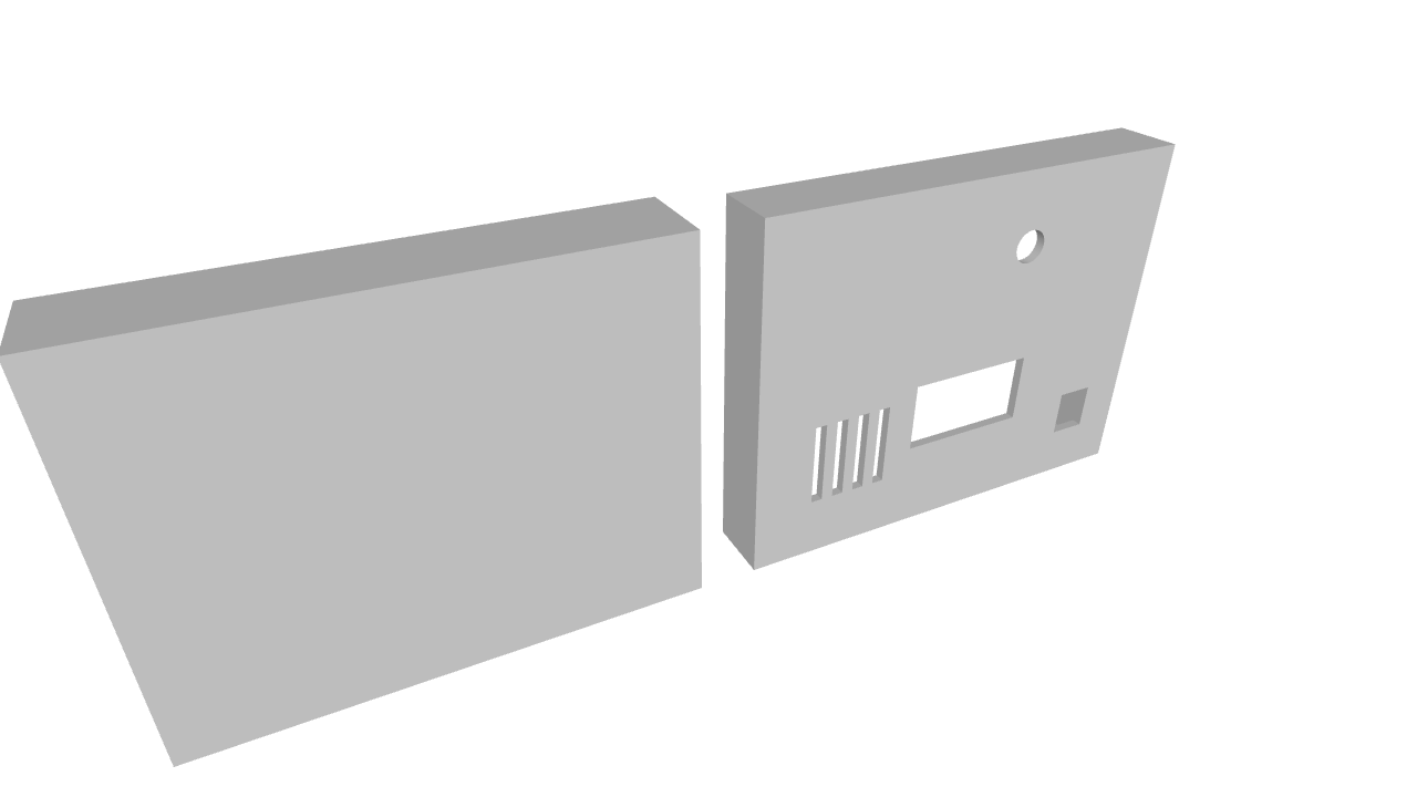
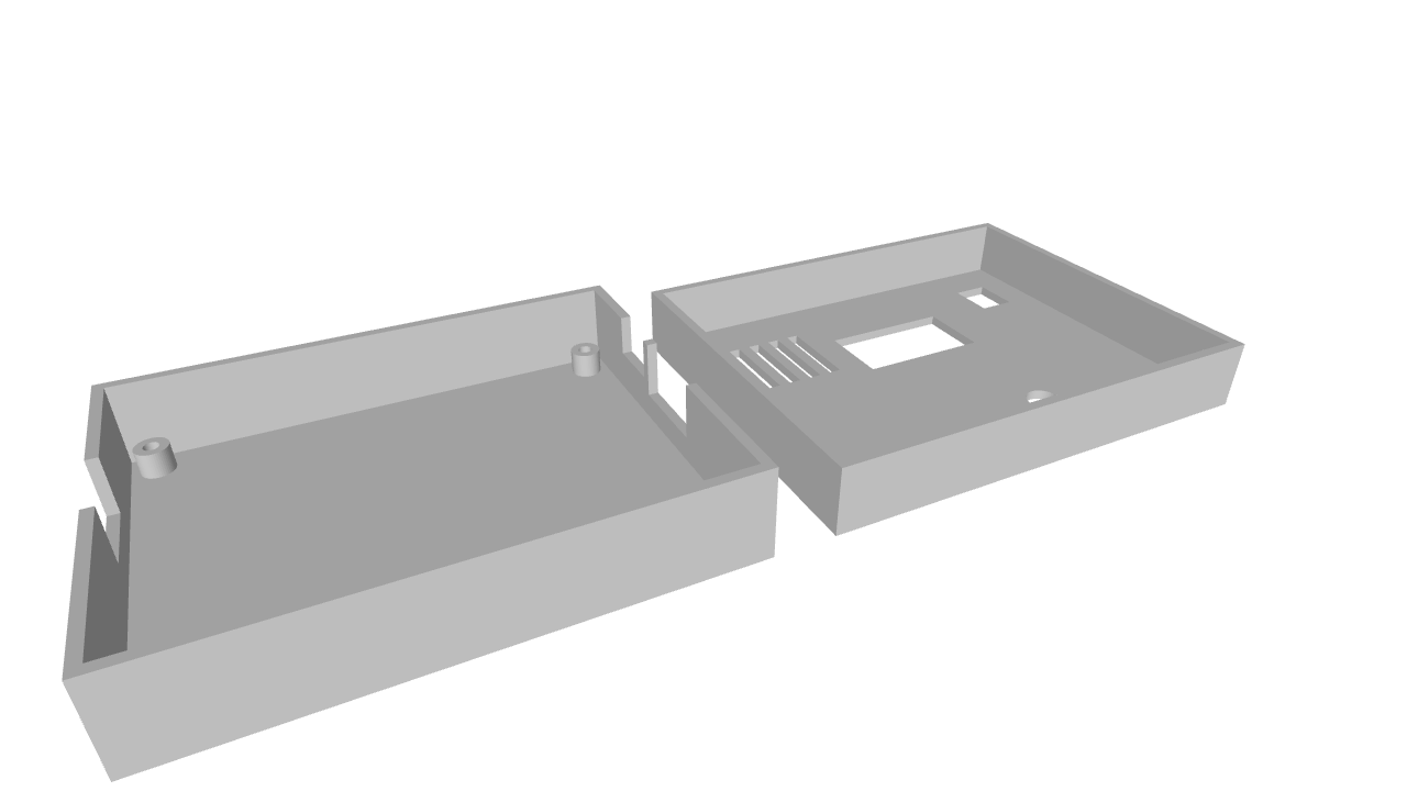
The electronics perform the measurement, the firmware handles the identification and calculations, and the OLED provides the user interface—but the enclosure is what turns all of those individual elements into a complete handheld instrument.
The result is a cleaner and more professional device that can be placed on an electronics workbench and used repeatedly without having exposed wires and modules getting in the way.
For makers, this is one of the most satisfying stages of a project: seeing a digital design become a real physical product.
And with PCBWay’s range of 3D-printing technologies and materials, the same approach can be extended far beyond this component tester—from sensor housings and robotic parts to custom instrument cases and functional prototypes.
Software and Firmware Overview
The firmware is built specifically around the resource limitations of the ATmega328P.
It uses AVR functionality for ADC operation, EEPROM, watchdog handling, interrupts and program-memory storage, along with the Wire and U8x8 libraries for the OLED interface.
One particularly interesting design choice is the use of U8x8 text mode for the SSD1306.
Instead of maintaining a conventional 128×64 full framebuffer, the firmware uses a text-oriented interface. This reduces memory requirements, which is important on an ATmega328P/Nano.
The firmware also uses EEPROM-related calibration data and several correction parameters, allowing the measurement system to compensate for characteristics of the physical hardware.
OLED User Interface
The 128×64 SSD1306 OLED serves as the primary user interface of the component tester, allowing the entire measurement process to be controlled and monitored without requiring a computer or additional display.
The firmware communicates with the OLED using the I²C interface, with the display configured at address 0x3C. Instead of using a conventional full-screen graphics buffer, the project uses the U8x8 text-oriented interface. This is particularly suitable for the ATmega328P because it significantly reduces the amount of RAM required by the display system while still providing enough flexibility for a compact measurement instrument.
The display is responsible for communicating several stages of operation to the user.
During startup, it presents the project branding. Once the tester is ready, it displays the LCR Meter interface. When a component is connected and the TEST button is pressed, the display changes to a testing status so the user knows that the measurement process is underway.
Once the analysis is complete, the OLED becomes the main results screen, presenting the detected component type together with its measured parameters.
Depending on the component, the information can include values such as:
- Resistance
- Capacitance
- Inductance
- Diode forward voltage
- Transistor type
- hFE
- VBE
- MOSFET/FET identification and related parameters
The firmware also contains custom OLED symbols for commonly displayed electronics terminology, including resistor, capacitor, diode, semiconductor and resistance symbols. This allows the results to remain compact and readable even on the relatively small 128×64 display.
The Startup Sequence
The startup screen is the first interaction the user has with the instrument, so the firmware gives it a dedicated initialization sequence.
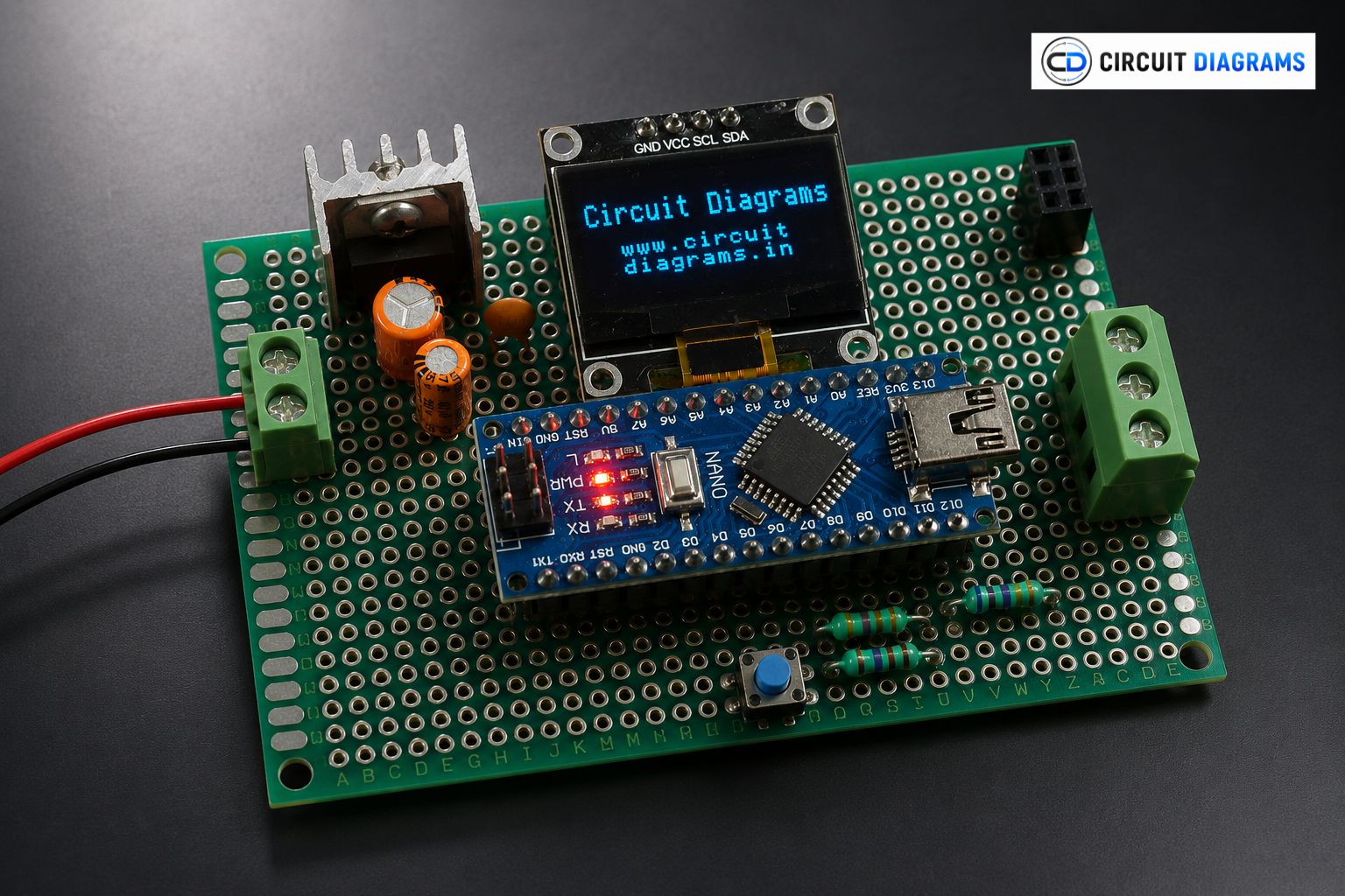
When power is applied, the microcontroller first initializes the OLED and prepares the custom characters used throughout the interface. Once the display is ready, the tester presents the project branding:
Circuit Diagrams
followed by:
www.circuitdiagrams.in
This short branding screen gives the DIY instrument a more finished and product-like feel instead of immediately jumping into the measurement interface.
The firmware keeps the branding screen visible for approximately 2.5 seconds before moving to the next stage of the startup sequence.
The display then shows:
LCR Meter
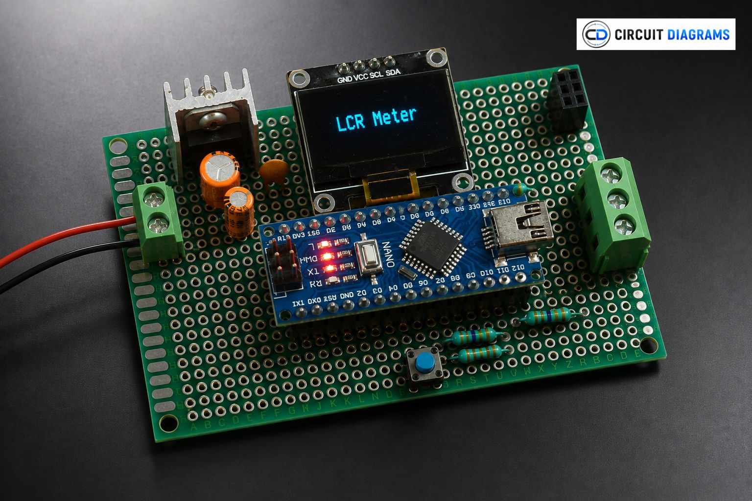
This acts as the transition between initialization and normal operation.
After the startup sequence has completed, the tester is ready for a component to be connected and tested.
Why the startup sequence matters?
Although a startup screen doesn’t affect the electrical measurement itself, it improves the overall user experience.
A well-designed instrument should communicate its state clearly:
Power On → Initialization → Branding → LCR Meter → Ready for Testing
Protecting the Tester From Charged Components
One of the most important precautions when using any component tester is also one of the easiest to overlook:
Never connect a charged capacitor directly to the tester.
A capacitor can retain electrical energy even after it has been removed from the original circuit. If that stored voltage is connected directly to the tester’s measurement terminals, it can interfere with the measurement and, depending on the voltage and stored energy, potentially damage the measurement circuitry.
For this reason, the firmware includes a voltage-detection and discharge sequence before carrying out the component analysis.
When a test begins, the firmware first checks the test terminals and attempts to remove any residual voltage. The three test points are configured through the measurement circuitry to provide a controlled discharge path, while the firmware monitors their voltage.
If an unexpected voltage is detected, the tester can stop the normal measurement process and display a warning such as:
Voltage Detected
Discharge First
This is an important feature because it provides the user with an additional warning before the measurement process continues.
Why automatic discharge is useful?
Without a discharge routine, a previously charged capacitor could still contain voltage when it is inserted into the tester.
The firmware therefore incorporates a sequence that:
- Checks the test terminals.
- Detects whether voltage is present.
- Provides a discharge path where appropriate.
- Monitors the voltage during the discharge process.
- Prevents normal testing when an unsafe voltage condition is detected.
This makes the measurement process more robust and reduces the likelihood of accidentally beginning a measurement with significant residual voltage on the test terminals.
But this is not a substitute for safe practice
The protection mechanism should not be treated as permission to connect externally powered circuits or high-voltage capacitors to the tester.
Before testing a component:
- Disconnect it completely from the circuit.
- Remove all external power.
- Discharge capacitors using an appropriate method.
- Verify that no significant voltage remains with a multimeter when necessary.
- Only then connect the component to the tester.
The firmware’s voltage detection and discharge routine should therefore be considered an additional layer of protection, not a replacement for proper electrical safety procedures.
For a DIY measurement instrument, this is an important distinction: the tester can help detect an unexpected voltage condition, but the safest workflow is always to make sure the component is safely discharged before connecting it in the first place.
Video Tutorial
Measurement Technology
How the Component Tester Works?
The tester uses the ATmega328P to analyze an unknown component through three test terminals: TP1, TP2 and TP3. These terminals are connected to the controller’s analog inputs, allowing the firmware to measure the voltage response of the connected component.
When a component is inserted, the firmware applies controlled measurement conditions and reads the resulting ADC values. It then uses these measurements to determine the electrical characteristics of the component.
The three-terminal arrangement is especially useful for transistors and FETs because the tester can examine different combinations of the three terminals instead of requiring the user to manually select a component type or pin configuration.
In simple terms, the process is:
Connect the component → Measure its electrical response → Identify the component → Calculate its value → Display the result.
Test Resistors and Why Calibration Matters?
Reference resistors are an important part of the measurement system because the tester uses known resistance values to calculate the value of an unknown component.
However, a resistor’s actual value is rarely exactly the same as its printed value. The firmware therefore provides separate low- and high-resistance reference values for each test terminal.
For example, the firmware contains:
RL_VALS[3]
RH_VALS[3]These values can be replaced with the actual resistance measured using a multimeter.
This is important because even small differences in the reference resistors can affect the calculated measurement. Using individually measured values helps the tester produce more consistent results across the three test terminals.
Calibration — The Key to Better Measurement Accuracy
Calibration allows the firmware to compensate for differences between the theoretical circuit and the actual hardware.
The project includes correction parameters for resistance, capacitance and inductance, along with individually calibrated reference-resistor values.
The most practical calibration step is to measure the reference resistors with a reliable multimeter and enter their actual values into the firmware.
This helps account for component tolerance and differences between the individual measurement channels.
Calibration does not make the tester a laboratory-grade instrument, but it can significantly improve the consistency of measurements from the actual hardware you have built.
How the Tester Determines the Component Type?
The tester doesn’t require the user to select whether the component is a resistor, capacitor or transistor.
Instead, the firmware examines the electrical response of the device and compares it with the characteristics expected from different component types.
The source contains dedicated detection modes for:
- Resistors
- Capacitors
- Diodes
- NPN transistors
- PNP transistors
- MOSFETs
- JFETs
What Happens When You Press the TEST Button?
Pressing TEST starts the complete automatic measurement sequence.
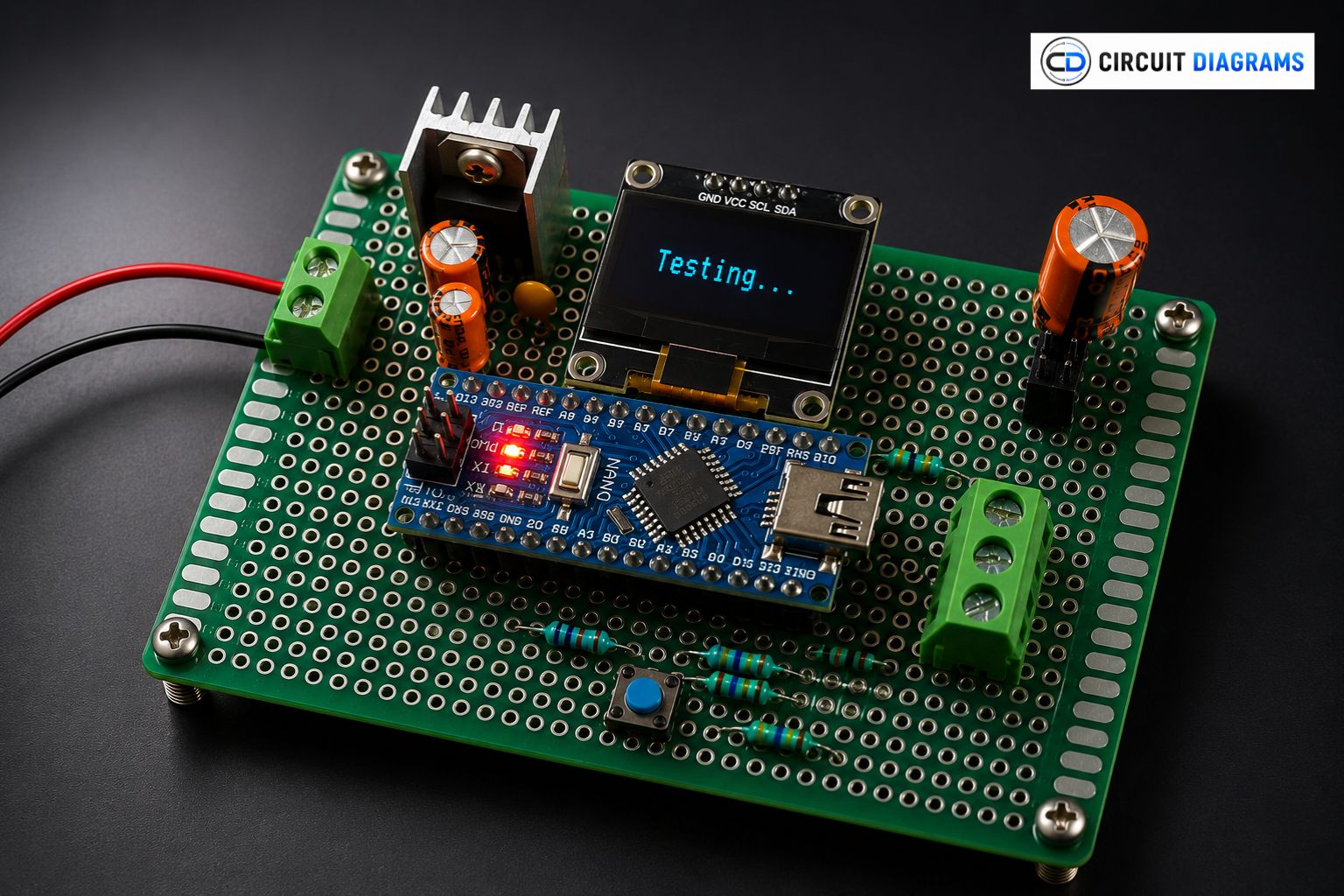
- The firmware first prepares the measurement system and clears the previous test state. It then checks and discharges the test terminals before beginning component detection.
- Next, the firmware examines different combinations of TP1, TP2 and TP3. It uses these measurements to identify semiconductor devices and determine their characteristics.
- If the component has not already been identified, the firmware proceeds with capacitance measurements and, where supported, inductance measurement.
- Finally, the detected component type and measurement value are sent to the OLED.
So from the user’s perspective, the entire process is simply:
Insert → Press TEST → Wait for analysis → Read the result.
Accuracy: What Can You Realistically Expect?
The accuracy of the tester depends on several factors, including:
- Reference-resistor tolerance
- ADC characteristics
- Calibration
- Wiring and contact resistance
- Component tolerance
- Temperature
- Semiconductor test conditions
This is why the firmware allows the reference resistors to be individually calibrated rather than relying only on their nominal values.
It is also important not to claim a specific accuracy percentage unless the finished hardware has been experimentally tested against a calibrated reference instrument.
For normal electronics work, the tester can be extremely useful for quick identification, component sorting and approximate measurement. When a measurement needs to be highly precise, it is best to verify the result using a good-quality multimeter or professional LCR meter.
The goal of calibration here is practical consistency—not laboratory-grade accuracy.
Component Testing
Testing Resistors
Connect the resistor between two test terminals and press TEST. The tester automatically measures and displays its resistance.
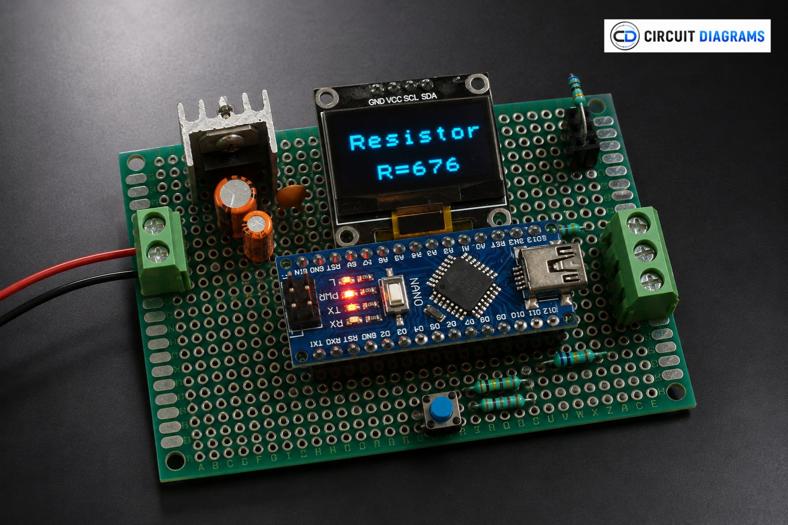
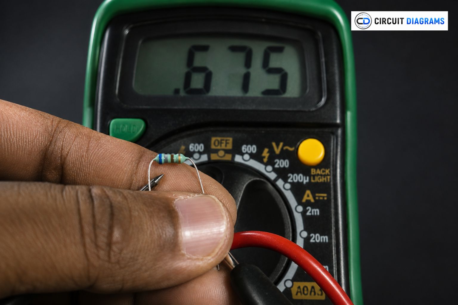
Then measure the same resistor with a multimeter in Ω mode. The readings should be close, but they don’t have to be identical because of resistor tolerance and measurement differences.
Testing Capacitors
Discharge the capacitor completely first.
Connect it to the tester and press TEST. The measured capacitance appears on the OLED.
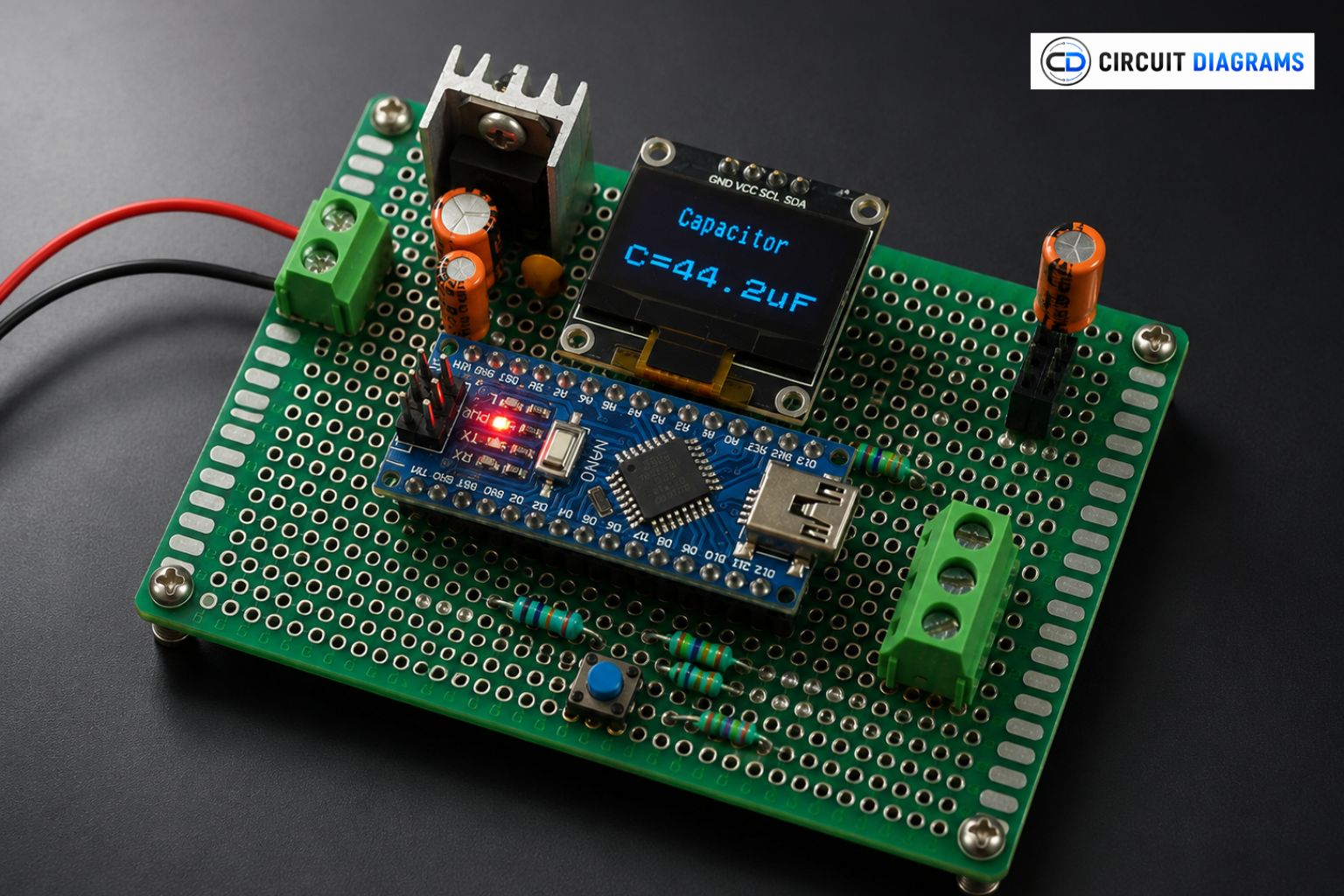
If your multimeter has capacitance mode, test the same capacitor and compare the readings. Small differences are normal because of component tolerance and different measurement methods.
Testing Inductors
Connect the inductor to the tester and run the test. Where inductance measurement is supported, the tester will display the measured value.
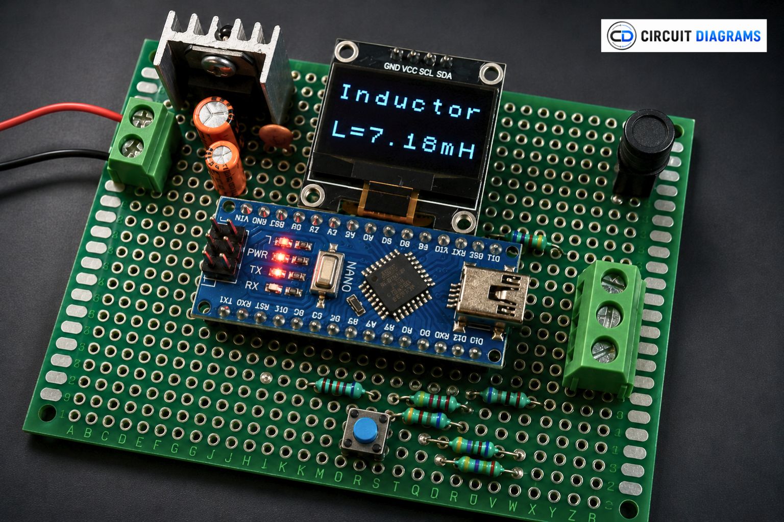
Compare it with an LCR meter or multimeter that specifically supports inductance measurement. Readings can vary with test frequency, winding resistance and parasitic effects.
Testing Diodes and LEDs
Connect the diode or LED and press TEST. The tester identifies the diode and displays its forward voltage (Vf).
You can verify it using a multimeter’s diode mode. Reversing the probes also helps confirm polarity.
Small differences in Vf are normal because the two instruments may use different test currents.
Testing Transistors — NPN and PNP
Connect the three transistor terminals and press TEST. The tester automatically identifies NPN or PNP and can display hFE and VBE.
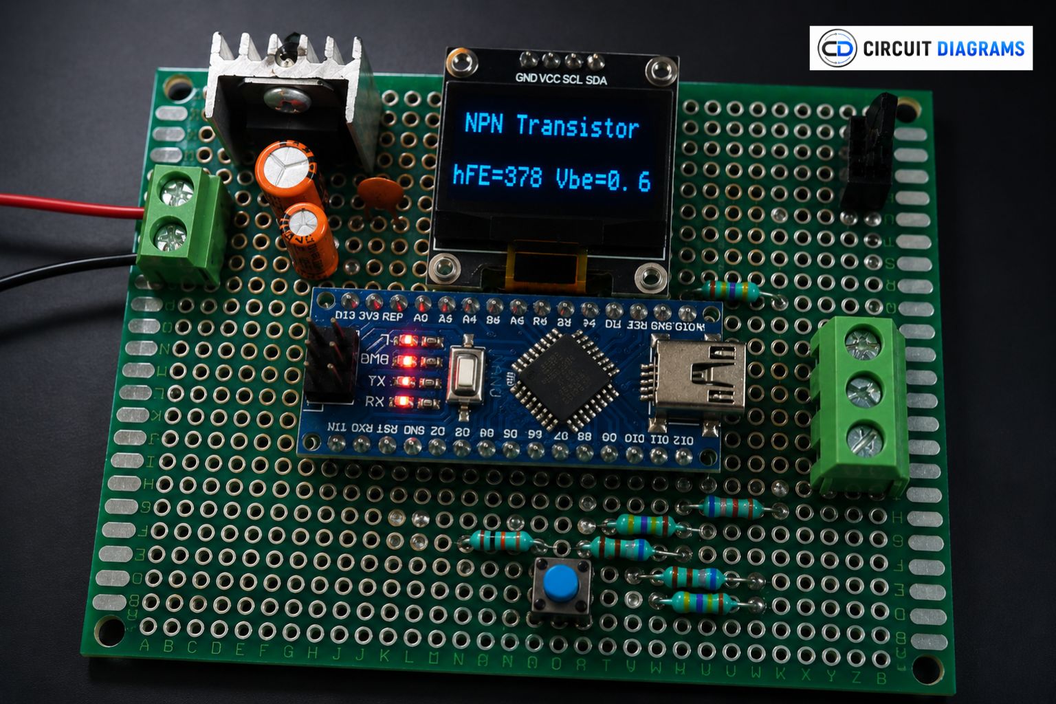
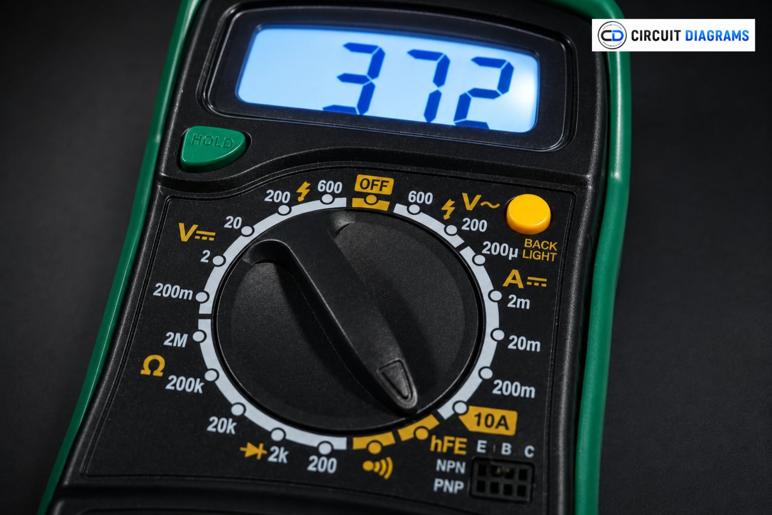
Use a multimeter’s diode mode to check the transistor junctions, or its hFE function if available.
hFE readings may differ because different instruments use different test currents.
Testing MOSFETs
Connect the MOSFET and run the test. The firmware can identify supported N-channel and P-channel MOSFETs and provide related measurement information.
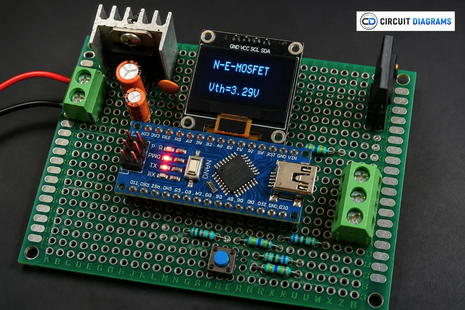
A multimeter can then be used to check the MOSFET’s body diode and look for shorts between terminals.
Troubleshooting the Component Tester
| Problem | Quick Checks |
|---|---|
| OLED not working | Check I²C wiring, confirm address 0x3C, and verify the OLED supply voltage. |
| Component not detected | Check the test-terminal connections, clean the contacts, and make sure the component is not connected to another circuit. |
| Incorrect capacitor reading | Fully discharge the capacitor, check its polarity if applicable, and repeat the measurement with short connections. |
| Incorrect transistor identification | Check the transistor orientation, clean the terminals, and compare the result with its datasheet. |
| MOSFET not detected correctly | Verify the pin connections, check the MOSFET datasheet, and test for shorts with a multimeter. |
| Unstable measurements | Clean the test contacts, keep wires short, and avoid touching the terminals during measurement. |
Practical Tips for Better Measurements
A few simple practices can make a noticeable difference:
- Always discharge capacitors before testing.
- Keep test wires and connections as short as practical.
- Clean oxidized or dirty test contacts.
- Use accurately measured reference resistors during calibration.
- Avoid touching sensitive measurement contacts while testing.
- Verify unusual readings with a reliable multimeter.
- For transistors and MOSFETs, check the datasheet and pin configuration before testing.
These small precautions help improve repeatability and prevent misleading results.
Advantages and Limitations
| Advantages | Limitations |
|---|---|
| Automatic component identification | Accuracy depends on calibration and hardware quality. |
| Supports multiple component types | Semiconductor readings depend on test conditions. |
| Compact Arduino-based design | Component tolerance can affect results. |
| OLED measurement display | Wiring and contact resistance can introduce errors. |
| Calibration capability | It is not a replacement for professional laboratory measurement equipment. |
| Three-terminal automatic testing | |
| Customizable hardware and firmware | |
| Custom 3D-printed enclosure |
Who Should Build This Project?
This project is ideal for electronics hobbyists, Arduino makers, students, repair enthusiasts and DIY instrument builders.
It is also a practical learning project because it combines several important electronics concepts in one device:
- ADC-based voltage measurement
- Component characterization
- Automatic component identification
- Calibration
- Embedded programming
- OLED interfacing
- Practical electronics testing
Possible Future Upgrades
The current design can also be expanded in several ways. Some possible future improvements include:
- ZIF socket for easier component insertion
- Rechargeable battery operation
- Improved 3D-printed enclosure
- More graphical OLED interface
- USB/serial measurement logging
- PC monitoring software
- Test-result storage
- Improved on-device calibration menu
These are future possibilities, not features of the current implementation.
Conclusion
This project combines an Arduino Nano, automatic component identification, ADC-based measurement, OLED feedback and calibration into a compact DIY test instrument.
From resistors and capacitors to diodes, transistors and MOSFETs, the tester can automatically analyze a wide range of components without requiring the user to manually select the measurement mode.
The custom 3D-printed enclosure, produced with the support of PCBWay, also takes the project beyond a simple breadboard experiment and gives it the appearance and usability of a proper bench instrument.
More importantly, building this project provides hands-on experience with embedded programming, ADC measurement, component characterization, calibration and practical electronics testing.
It is not intended to replace professional laboratory equipment—but as a DIY electronics workbench tool, it is a practical and rewarding project that you can build, calibrate and improve yourself.
FAQ — Frequently Asked Questions
What is an Arduino automatic component tester?
An Arduino automatic component tester is a DIY electronic instrument that uses an Arduino Nano and three test terminals to automatically identify and measure electronic components. Depending on the device, it can measure resistance, capacitance, inductance, diode forward voltage, and identify transistors and MOSFETs.
Can this component tester measure resistors?
Yes. Connect the resistor to the test terminals and press TEST. The tester automatically measures and displays its resistance. For verification, the same resistor can be measured with a multimeter in resistance mode.
Can it measure capacitors and inductors?
Yes. The tester supports capacitance measurement and inductance measurement where supported by the firmware. Capacitors should always be completely discharged before testing. Inductance readings can vary depending on the measurement conditions and component characteristics.
Can it test transistors and MOSFETs?
Yes. The tester can automatically identify supported transistor and FET types by analyzing their electrical behavior across the three test terminals. It can also provide parameters such as hFE and VBE for supported bipolar transistors.
Why should a capacitor be discharged before testing?
A capacitor can retain electrical energy even after being removed from a circuit. Connecting a charged capacitor can interfere with the measurement and may damage the tester. Always safely discharge the capacitor before connecting it to the test terminals.
Why does the component tester give a different reading from my multimeter?
Small differences can occur because of calibration, component tolerance, ADC characteristics, contact resistance and different measurement methods. For precision measurements, verify the result with a reliable multimeter or professional LCR meter.