
The objective of this project is to fully understand the 10’s complement using the 4-bit adder IC-7483. The IC-7483 is a commonly available TTL 4-bit parallel adder chip. It contains four inter-connected fully adders and a look-ahead carry circuitry for its operation.
The logic symbol of IC-7483 is shown in figure 2. It has two 4-bit inputs X3, X2, X1, X0 and Y3, Y2, Y1, Y0 and the carry input Cin in the LSB stage. The outputs are a 4-bit sum S3, S2, S1, and S0 and carry output Cout from the MSB stage. Two or more parallel adder blocks can be connected in a cascade to perform the addition operation on larger binary numbers. The four least significant bits of the number are added in the first adder.
The carry output of this adder is given as the carry input to the second adder, which adds the four most significant bits of the number. The output carries of the second adder is the final carry output.
Must Read 9’s Complement Circuit Using IC-7483
Project

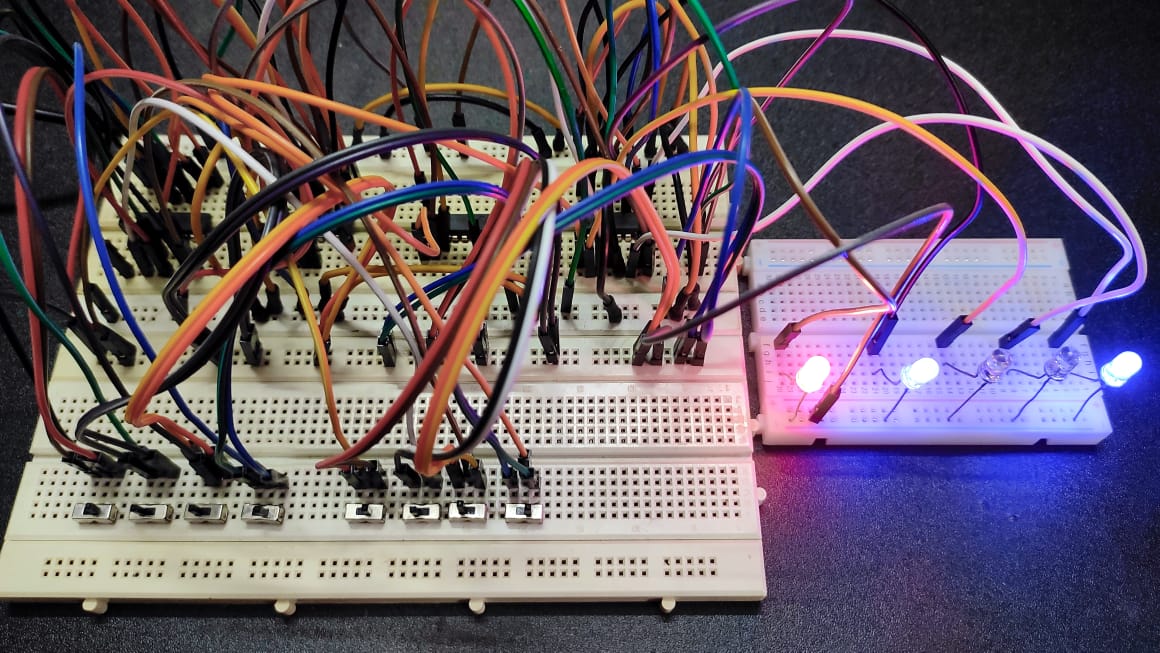
Circuit Diagram

Components Required
- 7483 Full Adder IC
- 7404 NOT Gate IC
- 3 Terminal Switch (x4)
- LED (x4)
- +5V Power Supply
- Breadboard
- Wires
About Parts of 10’s Complement Circuit
IC-7483 Full Adder (4-Bit Binary Adder)


The IC-7483 is a commonly available TTL 4-bit parallel adder chip. It contains four interconnected full adders; a look-ahead carry circuitry for its operation (CLA = Carry Look-Ahead Adder). The logic symbol of IC7483 is shown in fig 2 and the pin configuration in table 1. It has two 4-bit A3, A2, A1, A0 and B3, B2, B1, B0 and a carry input Cin in the LSB stage. The outputs are a 4-bit sum S3, S2, S1, S0 and a carry output (Cout) from the MSB stage.
Two or more parallel adder blocks can be connected in a cascade to perform the addition operation on a larger binary number. The four LSB of the number is added in the first adder. The carry output of this adder is given as carrying input to the second adder, which adds the four MSB of the number. the output carry of the second adder is the final carry output.
IC-7404 (NOT Gate IC)
The IC-7404 is a logic gate IC. It consists of six NOT gates. We know that the NOT gate is also called an inverter because it does complement of the inputs. When we apply zero or low signal to the input, it gives 1 or high signal as in the output. The pin diagram of the IC-7404 is shown in figure 4.
The general form of Truth Table for NOT gate is:
The truth table consists of input (x) and output as mod of |x̄|.
| Input (x) | Output (y) |
|---|---|
| 0 | 1 |
| 1 | 0 |
Circuit Connection for 10’s Complement Circuit
The circuit connection for this circuit is very easy because few components are used in this circuit. At first, we connect the pins I1, I2, I3 and I4 of the IC-7404 to the common terminals of the 3-terminal switch respectively. Then connect the pin B0, B1, B2, and B3 of the IC-7483 to the pin O1, O2, O3, and O4 of the IC-7404. Pin Cin is connected to the +Vcc and Cout is set to float for 10’s complement. Then apply +5V VCC across the A1 and A3 pins and ground to the A0 and A3 pins of the IC-7483.
Working Principle of 10’s Complement Circuit
Now to get 10’s complement using a 4-bit full adder i.e., IC-7483 have some specific ways.
- 10’s complement of a 4-bit number (BCD code) “x” is, 1010-x = 10-x; or simply we can add (+1) to the result out for the 9’s complement.
- The 10’s complement of a BCD code of a number “x” can be expressed as:
9-x+1 = (15-6)-x+1 = (15-x)-6+1 = x̄-6+1=(x̄+10)+1
or, (x̄+11)
- The first part is the 9’s complement of “x” when “x” is a BCD number i.e. (15-x) produces x̄.
- And the (+1) is added to it when the Cin input of the full adder IC-7483 is connected to logic high i.e., 1 or +Vcc.
Truth Table for Full Adder
| A | B | CIN | SUM | CARRY (COUT) |
|---|---|---|---|---|
| 0 | 0 | 0 | 0 | 0 |
| 0 | 0 | 1 | 1 | 0 |
| 0 | 1 | 0 | 1 | 0 |
| 0 | 1 | 1 | 0 | 1 |
| 1 | 0 | 0 | 1 | 0 |
| 1 | 0 | 1 | 0 | 1 |
| 1 | 1 | 0 | 0 | 1 |
| 1 | 1 | 1 | 1 | 1 |
Truth Table for 10’s Complement
| Digits | X3 | X2 | X1 | X0 | S3 | S2 | S1 | S0 |
|---|---|---|---|---|---|---|---|---|
| 0 | 0 | 0 | 0 | 0 | 1 | 0 | 1 | 0 |
| 1 | 0 | 0 | 0 | 1 | 1 | 0 | 0 | 1 |
| 2 | 0 | 0 | 1 | 0 | 1 | 0 | 0 | 0 |
| 3 | 0 | 0 | 1 | 1 | 0 | 1 | 1 | 1 |
| 4 | 0 | 1 | 0 | 0 | 0 | 1 | 1 | 0 |
| 5 | 0 | 1 | 0 | 1 | 0 | 1 | 0 | 1 |
| 6 | 0 | 1 | 1 | 0 | 0 | 1 | 0 | 0 |
| 7 | 0 | 1 | 1 | 1 | 0 | 0 | 1 | 1 |
| 8 | 1 | 0 | 0 | 0 | 0 | 0 | 1 | 0 |
| 9 | 1 | 0 | 0 | 1 | 0 | 0 | 0 | 1 |
Example


Precautions & Discussions of 10’s Complement Circuit
- Various resistance should be chosen in the conduction state current through the LEDs. So that it does not exceed the maximum rated current. So carefully choose the safety resistance for LED.
- The experiment has been done by using the level logic where a high voltage i.e. equal to (+Vcc) i.e. =+5V DC is taken as ‘1’ and a low voltage i.e., equal to (GND) = 0V is taken as ‘0’.
- LEDs used for proper current limiting resistance can be used for easy and quick visual identification of the ‘0’ and ‘1’ state. If a LED glows then it is a 1’s state and if it does not glow then it is a ‘0’ state.
- While connecting the +5V DC supply to the IC, special care should be taken. Connection to any wrong pin may damage the IC.
- Carefully connect the (Cin) pin for IC-7483 (4-bit full adder) for 10’s complement; as for 10’s compliment Cin =1 or high voltage level.
- For connecting the inverted output from NOT Gate, IC-7404 to IC-7483 one of the 4-bit inputs, special care should be taken during setting up the wire connection to LSB and MSB bit. So that the output should be in the correct form otherwise it goes wrong.


Thanks it really helps for my practical.