BCD subtractor is a circuit which accepts minuend and subtrahend in the form of BCD and produces the difference in BCD form. The BCD subtractor will be implemented in this project with the help of a BCD adder and 9’s complement circuits. A schematic diagram of the design of the BCD Subtractor is shown in figure (1).
Must Read BCD Adder Circuit
Project

Circuit Diagram
Components Required
- 7483 4 Bit Adder (x4)
- 7404 NOT Gate (x2)
- 7432 OR Gate
- 7485 Magnitude Comparator
- 7486 EX-OR Gate
- Single Pole 2-Way Switch (x8)
- LED (x5)
- 5V Power Supply
- Breadboard
- Wires
About Parts of BCD Subtractor Circuit
IC-7486 EX-OR Gate

This is a Quad 2-input EX-OR gate with 14 pins IC. It is widely used in the arithmetic section of a computer. This gate is widely used in digital electronics design and therefore, is available in IC form. EX-OR has two inputs and an output. Output is 1 (High) only when the inputs are unequal and output is 0 (Low) when the inputs are the same. If this acts as an inequality detector. The pin diagram of the IC-7486 is shown in figure (2).
The Truth Table for IC-7486 X-OR Gate
| A | B | Y=A⊕B |
|---|---|---|
| 0 | 0 | 0 |
| 0 | 1 | 1 |
| 1 | 0 | 1 |
| 1 | 1 | 0 |
IC-7483 4-Bit Full Adder
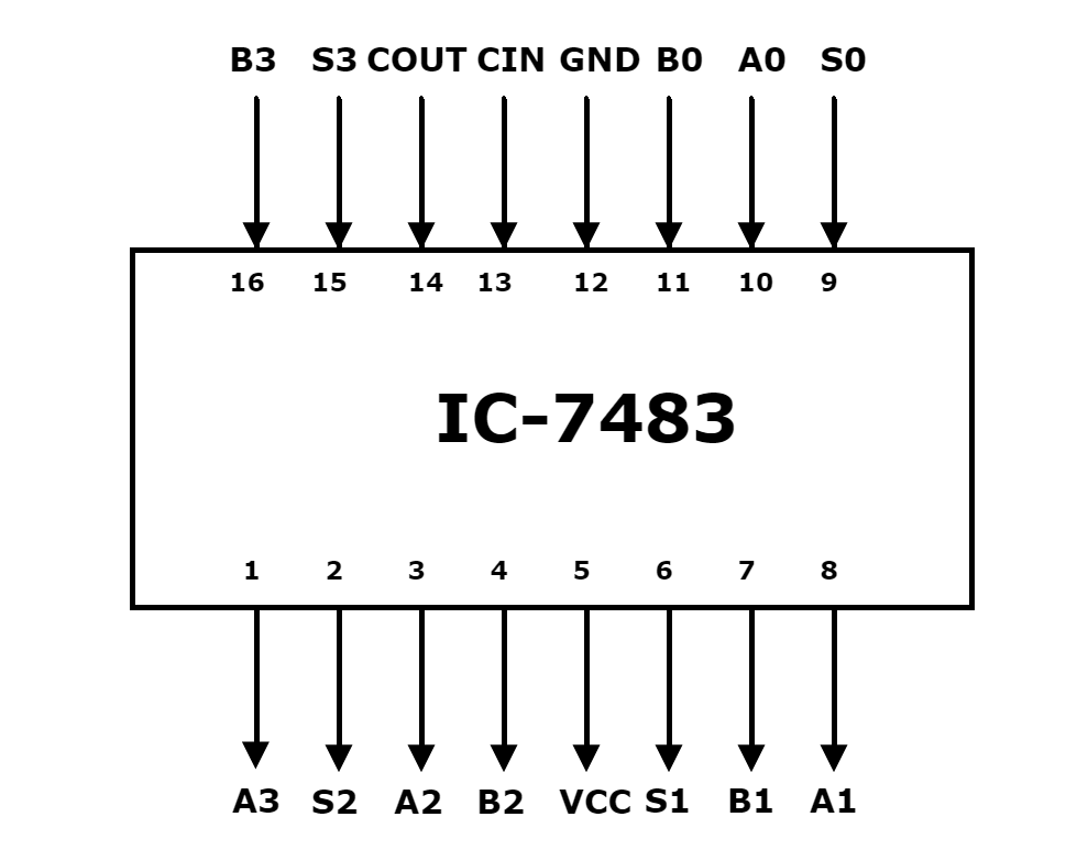
The IC-7483 is a commonly available TTL 4-bit parallel adder chip. It contains four interconnected full adders; a look-ahead carry circuitry for its operation (CLA = Carry Look-Ahead Adder). The logic symbol of IC-7483 is shown in figure (3) and the pin configuration in table 1. It has two 4-bit A3, A2, A1, A0 and B3, B2, B1, B0 and a carry input Cin in the LSB stage. The outputs are a 4-bit sum S3, S2, S1, S0 and a carry output (Cout) from the MSB stage.

Two or more parallel adder blocks can be connected in a cascade to perform the addition operation on a larger binary number. The four LSB of the number is added in the first adder. The carry output of this adder is given as carrying input to the second adder, which adds the four MSB of the number. the output carry of the second adder is the final carry output.
IC-7404 NOT Gate

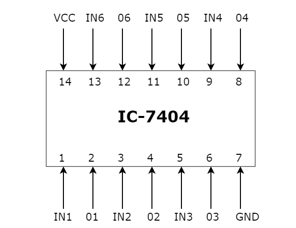
The IC-7404 is a logic gate IC. It consists of six NOT gates. We know that the NOT gate is also called an inverter because it does complement the input. When we apply zero or low signal to the input, it gives 1 or high signal as in the output. The pin diagram of the IC-7404 is shown in figure (4).
The Truth Table for IC-7404 NOT Gate
| Inputs | Outputs |
|---|---|
| X | x̄ |
| 0 | 1 |
| 1 | 0 |
IC-7485 4 bit Comparator

The IC-7485 is a 4-bit magnitude comparator of the TTL family. This IC compares the magnitudes of two 4-bit numbers; A3, A2, A1, A0. and B3, B2, B1, B0. This IC has three outputs (A>B)out, (A=B)out, and (A<B)out. Besides those pins, this IC has cascading facilities. These cascading inputs are (A>B)in, (A=B)in, and (A<B)in. When the two inputs are equal then the outputs of the chip become a function of cascading inputs.
IC-7432 OR Gate

The IC-7432 is a member of gate ICs and has the functionality of an OR gate or function. It will give a high if either all or any one of the two inputs is high. IC-7432 has 4 OR gates of 2 inputs in 1 package. The internal gates are made of from Schottky Transistor of low power.
Circuit Connection for BCD Subtractor Circuit
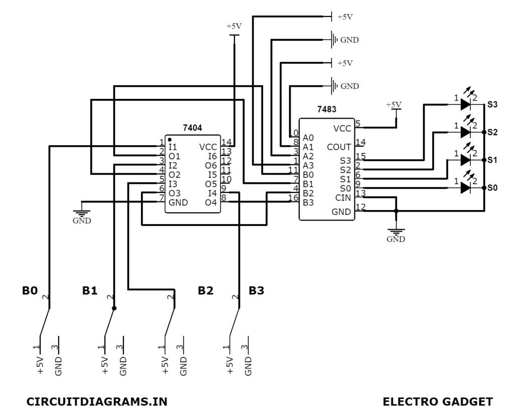
- Firstly, for the 1st 9’s complement circuit we use the NOT Gate (IC-7404) and CLA (carry look-ahead) Adder IC (IC-7483).
- Secondly, for the middle BCD Adder part, we use two (IC-7483) CLA Adder, (IC-7485) 4-bit Magnitude comparator and one (IC-7432) OR Gate.
- Thirdly, for the last part i.e. 2nd 9’s complement circuit, we use the X-OR Gate (IC-7486) and CLA Adder IC (IC-7483).
Working Principle of BCD Subtractor Circuit
The working principle of this project is quite complicated, so read this carefully. In subtractor, one 9’s complement circuit is used to produce the 9’s complement of the BCD subtrahend Y (Y3 Y2 Y1 Y0). The output of the 9’s complement circuit is used as one of the two inputs of the BCD adder. The other input of this BCD adder is connected directly to the BCD minuend. The second 9’s complement circuit is connected to the sum of the output of the BCD adder which generates the 9’s complement of the BCD adder output if the EN(=Cout) input of the second 9’s complement circuit is 1 otherwise for EN=0 i.e., Cout = 1, the 9’s complement circuit passes the sum output of the BCD adder unchanged. This type of 9’s complement circuit is shown below.

The action of this single-decade BCD subtractor can be understood from the following discussion.
There may be two cases that may arrive:
- BCD minuend (X) ≤ BCD subtrahend (Y)
- BCD minuend (X) > BCD subtratend
In both cases,
An input of the BCD adder = Minuend = X
B input of the BCD adder = 9’s complement of the subtrahend = 9-Y
Case (1): X≤Y
The sum output of the BCD adder. Then X + (9- Y) + Cin + BCD correction factor (if needed).
As X≤Y, the sum X+ (9-Y) can never exceed 9 because the maximum value of X and y is 9.
Therefore, carry output from the BCD adder = Cout=0 and hence, carry input Cin is 0 and as Cin and Cout are connected.
The BCD correction in the adder unit is not needed when Cout = 0 because the sum from the full adder unit of this BCD adder is X+(9-Y)≤9.
The enable input (EN) of the second 9’s complement circuit = Cout=1, so the output of the second 9’s complement generator circuit is 9-{X+(9-Y)} = (Y-X).
Hence, the output of the 9’s complement circuit gives the magnitude and the output of the NOT Gate is 1. This output indicates the negative sign.
Case (2): X>Y
In this case, the sum X+(9-Y) always exceeds 9, so the BCD correction factor within the BCD adder will be 6.
Carry output from the BCD adder is Cout=1 and hence the Cin=1.
Sum output of the BCD adder= X+(9-Y) +1+6 = (X-Y)+16.
Factor 16 indicates that Cout=1. If this Cout is ignored then the sum output from the BCD adder will be (X-Y) and as Cout=1, the enable input of the second 9’s complement circuit is 0. Therefore, the output of this 9’s complement circuit will be (X-Y).
The Theoretical Truth Table for the subtraction of two BCD numbers and getting the result in BCD
| X3 | X2 | X1 | X0 | Y3 | Y2 | Y1 | Y0 | EN (sign) | S3 | S2 | S1 | S0 |
| 0 | 0 | 1 | 1 | 0 | 0 | 1 | 0 | 0 | 0 | 0 | 0 | 1 |
| 1 | 0 | 0 | 0 | 0 | 0 | 1 | 1 | 0 | 0 | 1 | 0 | 1 |
| 1 | 1 | 1 | 1 | 0 | 0 | 1 | 0 | 0 | 1 | 1 | 0 | 1 |
| 1 | 1 | 0 | 1 | 0 | 0 | 1 | 1 | 0 | 1 | 0 | 1 | 0 |
| 0 | 0 | 1 | 1 | 1 | 1 | 1 | 1 | 1 | 1 | 1 | 0 | 0 |
| 0 | 0 | 0 | 1 | 1 | 0 | 1 | 1 | 1 | 1 | 0 | 1 | 0 |
| 0 | 0 | 0 | 0 | 0 | 0 | 0 | 1 | 1 | 0 | 0 | 0 | 1 |
| 0 | 0 | 1 | 0 | 0 | 1 | 1 | 0 | 1 | 0 | 1 | 0 | 0 |
Precautions & Discussions for BCD Subtractor Circuit
- Various resistance should be chosen in the conduction state current through the LED. So that it doesn’t exceed the maximum rated current. So carefully choose the safety resistance.
- The experiment has been done by using +ve level logic where a high voltage i.e. equal to (+VCC) i.e., +5V is taken as ‘1’ and a low voltage i.e., equal to GND i.e., 0V is taken as ‘0’.
- LEDs with proper current limiting resistance can be used for easy, quick and visual identification of ‘0’ and ‘1’ states. If the LED glow then it is in an on state and if it doesn’t glow then it is in an off state.
- While connecting the 5V DC supply to the IC special care should be taken. Connection to any wrong pin any damage maybe happen.
- Carefully connect the pins bitwise from comparators IC-7485 and IC-7483. For any wrong correction, the output will not be as we want to get.
- For the BCD Subtractor circuit, we are using two 9’s complement circuits, one at the first point i.e., before the BCD adder and the other just after the BCD adder circuit.
- Special care should be taken during setting up the wire connection to LSB and MSB bit so that the output should be in the correct form otherwise it goes wrong.
