A voltage doubler circuit is a type of electronic circuit that charges capacitors through input voltage and switches these charges twice the voltage produced at the output as at its input.
Practically, a conventional power supply produces a 230V AC supply which can be used for multiple electrical and electronic loads. But, a few loads of electronic equipment require a higher voltage to operate like cathode ray tubes, X-Ray, water pumps, lasers, travelling wave tubes and so on. So the available voltage needs to be multiplied using the voltage multiplier device. The voltage multiplier is an electronics circuit containing capacitors and diodes that can be used for increasing the voltage i.e. double the applied voltage. There are some types of voltage multipliers such as voltage doubler, voltage more triple, and voltage quadruple.
Must Read Top 555 Timer Hobby Projects
What is a Voltage Doubler?
A voltage doubler circuit is defined as an electronic circuit that doubles the applied voltage by using the charging and the discharging principle of capacitors. It consists of two main electronic components like capacitors and diodes.
It can be also defined as a rectifier that takes an input AC voltage and produces an output DC voltage that is approximately double the input voltage. Even though there is a DC-to-DC voltage doubler, in this type of voltage doubler circuit driving circuit is required for switching control.
There are different types of voltage doubler circuits available such as simple voltage doubler, 555 timer-based voltage doubler circuit, voltage doubler rectifier like Villard circuit, Greinacher circuit, bridge circuit, switched capacitor circuits, Dickson charge pump, cross-coupled switched capacitors.
Project

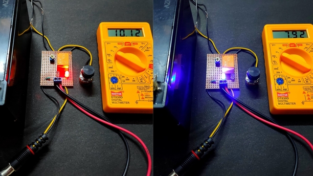
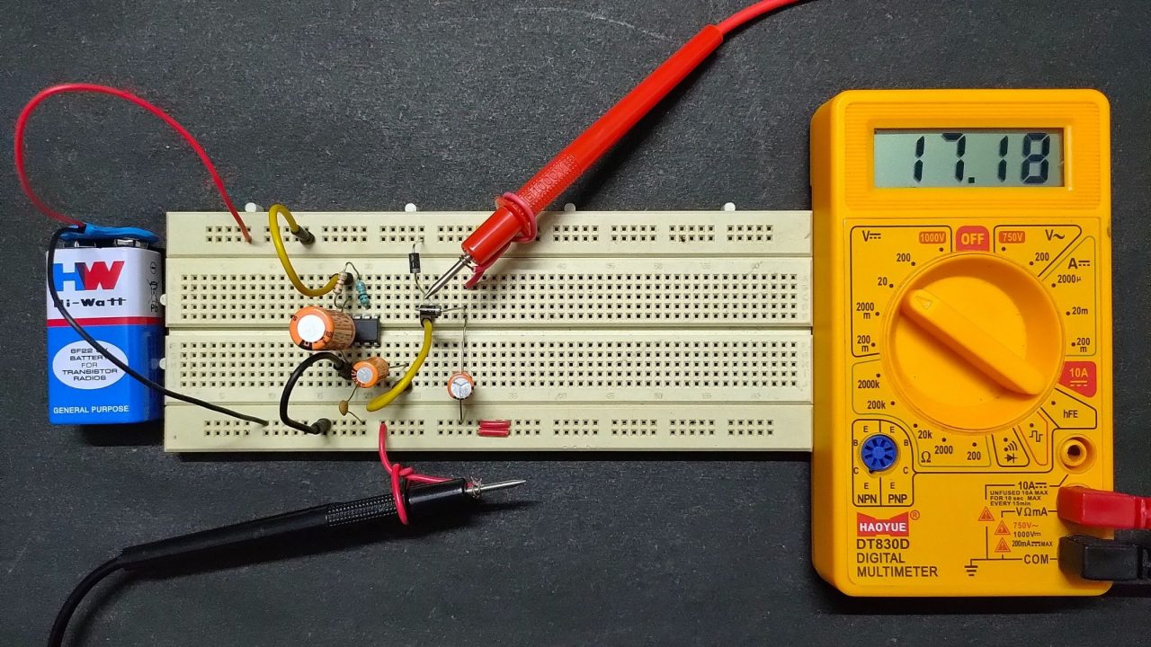
This project will learn how to make a DC Voltage Doubler Circuit using a simple 555 timer IC, diodes, and capacitors. This circuit operates around 5V to 15V DC voltage and produces double the input voltage at the output. For example, if the input voltage is 5V, the output voltage will be approximately 10V.
It produces a square wave frequency of around 2KHz with the help of resistors and capacitors. The forward-biased diode D2 and a 100uF capacitor are connected such for amplifying the signals. The diode D1 prevents the complete discharge of the capacitor C3.
Circuit Diagram

Components Required
- NE555 Timer IC
- 1N4007 PN Diode (2x)
- 1000μF/35V Capacitor
- 100μF/35V Capacitor (2x)
- 0.01μF Ceramic Capacitor (Code: 103)
- Resistor (4.7KΩ, 2.2KΩ, 10KΩ)
- Red LED
- Wires
Circuit Connection
The positive connection is (+) and the negative connection is (-) the power supply. The 555 timer works here as an astable mode. To make the power supply smooth and stable, we connect a 1000μF/35V capacitor between the (+ve) and (-ve) terminals of the input. Connect pins 4 and 8 to (+ve) and pin 1 directly to the ground.
Connect a 4.7KΩ resistor between the (+ve) and pin 7 of the 555 timers ic. Also, connect a 10KΩ resistor between pins 7 and 6. Therefore connect pins 2 and 6 and ground through a 0.01μF ceramic capacitor.
At the output section, connect a 100μF/35V capacitor with the output pin 3 of the 555 timers ic. Therefore connect the (+ve) terminal of the capacitor between two 1N4007 diodes which are in series. Another 100μF/35V capacitor is used here for filtering the output voltage.
Working Principle of Voltage Doubler Circuit
The 555 timer IC, in combination with the 100μF capacitor, produces a square wave at its output. A square wave frequency means that the signal continuously alternates between positive voltage and negative voltage. For example, if the input voltage is 5V, the output voltage of 555 timer ic will be 0V for some time. Then set to 6V and stay at this voltage for some time, again set to 0V and so on. We added a 100μF capacitor with its negative terminal connected to the output of the 555 timers ic and its positive terminal connected to the positive terminal via a diode.
We need to add a 100μF capacitor with its negative terminal connected to the output of the 555 timers ic and its positive terminal connected to the positive terminal via a diode.
The logic behind the arrangement is that when the 555 timer ic output is at 0V (-ve), the 100μF capacitor charges through the 1N4007 diode. The voltage of the capacitor gets charged, which is equal to the applied voltage. It means that the forward bias voltage of the diode is approximately equal to the positive voltage of the applied voltage. When the output of the 555 timer ic is at (+ve), the voltage across the 100μF capacitor will be in series with the output of 555 timer ic.
Since two voltage sources are in series, the voltage on the other hand of the 100μF capacitor will be equal to the voltage at the output of 555 timer ic plus the voltage across the capacitor. Also, the output voltage of 555 timer ic and the voltage across the 100μF capacitor is equal to the (+ve) voltage of the power supply. The final voltage will be double the input voltage. The voltage at the n-junction of the diode is more than the p-junction, as a result, no current flows back to the positive terminal.
Now we have a double voltage than the input voltage. Another 1N4007 p-n diode is added to prevent the current from flowing through the capacitor from the output. In the end, a 100μF capacitor is connected to filter the output.
Applications of Voltage Doubler Circuit
- Voltage Doubler Circuits are normally used in micro ovens where higher amounts of voltages are required and there is no use of a transformer.
- Generally usable for generating voltages that generate strong electric fields in cathode-ray tubes.
- Used in low voltage sources where a higher amount is needed.