Overview of Conventional FPGA Design Tools
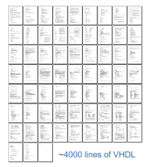
Over the first 20 years of FPGA development, hardware description languages (HDLs) like VHDL and Verilog evolved to become the primary languages for designing the algorithms that run on the FPGA chip. With the knowledge that you are constructing a circuit on an FPGA, these low-level languages incorporate some of the benefits of existing textual languages. Signals from external I/O ports must be mapped or connected to internal signals before being sent to the functions that house the algorithms in order to use the resulting hybrid syntax. These concurrently operating processes have the ability to refer to other FPGA-based operations. However, a sequential line-by-line flow makes it challenging to comprehend the true parallel nature of the job execution on an FPGA. Although HDLs share some characteristics with other textual languages, they also differ significantly because they are built on a dataflow model, in which I/O is linked to a number of function blocks through signals.
It is common practice to develop test benches in HDL that wrap around and exercise the FPGA design by asserting inputs and analyzing outputs in order to later verify the logic that an FPGA programmer created. A simulation environment is used to run the test bench and the FPGA code. This environment simulates the hardware timing behaviour of the FPGA chip and shows the designer all input and output signals for test validation. It frequently takes longer to create the first FPGA HDL design than it does to construct the HDL test bench and run the simulation.
The text-based logic must be converted into a configuration file or bitstream by a compilation tool via a series of intricate steps. This bitstream or configuration file specifies how the components should be connected. This is carried out after creating and testing an FPGA design using HDL. You frequently need to define a mapping of signal names to the pins on the FPGA device you’re utilizing as part of this multi-step manual process.
Programming FPGAs with VHDL
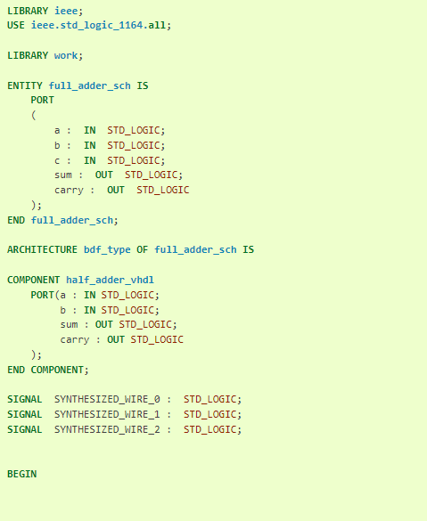
FPGA series like Zynq-7000 SoC, FPGA Spartan-7, Artix-7 FPGA, Virtex-7 FPGAs, and Kintex-7 FPGAs all use VHDL language to describe digital electrical circuits at different levels of abstraction. The abbreviation VHDL stands for Very High-Speed Integrated Circuits Hardware Description Language. This implies that VHDL can speed up the design process. It cannot be emphasized enough that VHDL is NOT a programming language. Because of this, knowing its syntax does not imply being able to build digital circuits using it. The HDL (Hardware Description Language) known as VHDL can be used to describe both synchronous and asynchronous circuits.
Like most popular programming languages, VHDL specifically allows the specification of a circuit’s functioning through directives. This enables more than only the structural description of a circuit (from simpler subcircuits). An HDL uses a description language that is very similar to software description languages to mimic the logical behaviour of a circuit. Digital circuits specified in VHDL can be simulated using simulation tools that faithfully reproduce the circuit’s behaviour. For this, programmers use a set of IEEE-standard rules that spell out the syntax of the language and how to simulate it. The VHDL code can also be downloaded as a file and used to program a reconfigurable device using a variety of applications that convert VHDL code. This process is known as synthesis. A specific tool completes the synthesis process in a manner that differs significantly from how other synthesis tools complete it.
Programming FPGAs with Verilog
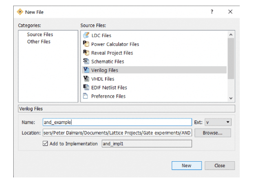
Verilog is a hardware description language (HDL). The most popular language for programming FPGAs is this one, followed by its competitor VHDL. When you can program an FPGA using a schematic that you are probably already familiar with and understand, why would you want to learn a challenging programming language? In reality, as designs become more complicated, representing them in a programming language is actually easier than drawing them. Like programming languages, Verilog incorporates elements like “if” statements, code blocks, and the capacity to add and subtract numbers.
Overview of High-Level Synthesis Design Tools
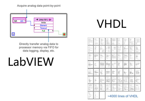
The creation of graphical HLS design tools like LabVIEW has removed some of the greatest obstacles to the standard HDL design process. Users with both knowledge and little experience in typical FPGA design techniques can make use of FPGA technology because parallelism and data flow are clearly depicted in the LabVIEW programming environment. To maintain previous intellectual property (IP), you may also utilize LabVIEW to incorporate pre-existing VHDL into your LabVIEW FPGA designs. Because LabVIEW FPGA is so tightly associated with hardware, unlike many HLS code generators, there is no need to rewrite code in VHDL to satisfy temporal or resource constraints.
In order to simulate and test the behaviour of your FPGA logic, LabVIEW offers features right in the development environment. Without knowing the low-level HDL language, you can still construct test benches to evaluate the logic of your design. Additionally, the adaptability of the LabVIEW environment enables more seasoned users to model the timing and logic of their designs by exporting them to cycle-accurate simulators like Xilinx ISim. You can start the compilation process with the push of a button and receive reports and any errors, if any, when compilation stages are complete thanks to the automation provided by LabVIEW FPGA compilation tools. To expedite the debugging process, LabVIEW graphically displays these key paths if your FPGA design does result in timing problems.
Programming FPGAs with LabVIEW
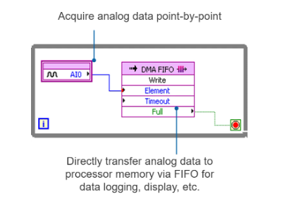
The ease of graphical creation of counters in LabVIEW makes them a perfect fit for FPGA implementation. I/O nodes can be used in LabVIEW FPGA to generate Analog signals and carry out Analog measurements. Unlike CPUs, FPGA hardware supports true parallel code execution, and LabVIEW FPGA has graphical loop structures to support the simultaneous execution of multiple block diagram elements. LabVIEW FPGA enables hardware execution of graphical block diagrams on the order of microseconds and nanoseconds.
Learn about the single-cycle Timed Loop, a special LabVIEW FPGA structure that allows any FPGA design to be optimized for size and speed. Mechanical switches and relays typically bounce when changing states. Debounce circuitry can be built using LabVIEW FPGA to filter out undesired digital edges. Shift registers and Feedback Nodes are now available in LabVIEW FPGA to send data over numerous loop cycles. Case structures can be used to selectively activate various FPGA design components, making them helpful for creating custom hardware triggers and state machines.
You can construct different timing engines in hardware using LabVIEW FPGA to achieve genuinely independent operation. The majority of data collection equipment is made to share sample clocks and triggers.
Conclusion
As a result of cutting-edge tools like LabVIEW making FPGAs more accessible, FPGA technology is now being employed more frequently. Examining the FPGA’s core operations and comprehending the level of block diagram translation into silicon for execution is still critical. Comparing and selecting hardware targets based on flip-flops, LUTs, multipliers, and block RAM is the simplest method for identifying the optimum FPGA chip for your application. Understanding resource utilization is very useful while developing, especially when optimising for size and performance.
